Special futures
Thickness: 1.6mm
Application: projector or projecting apparatus
Minimum trace size: 0.1mm
Minimum drill: 0.15mm
With blind and buried holes
Layers: 1 to 28
Board finished thicknesses: 0.2 to 7.0mm
Materials: FR-4, CEM-3, high Tg, halogen-free FR4 and Rogers,F4B
Maximum finished board size: 580 x 900mm
Minimum hole size: 4mil (0.1mm)
Minimum trace width/space: 3.5/3.5mil
Surface finishes/treatments: HASL, lead-free HASL, immersion gold, gold plating, immersion silver, immersion tin and OSP
Copper thicknesses: 0.5 to 6oz
Solder mask colors: green, yellow, black, white, red and blue
Copper thickness in hole: >18um
Inner packaging: plastic bag (vacuum packing)
Outline tolerance: ¡À0.13mm
Hole size tolerance: (PTH) ¡À0.076 and (NPTH) ¡À0.05mm
With UL and TS16949:2002 marks
Special requirements: buried and blind vias, impedance control, via plug, BGA soldering and gold finger
Profiling: punching, routing, V-cut and beveling
OEM services to all sorts of printed circuit board assembly as well as electronic encased products are provided.
6 layer hight PCB, OEM design PCB
1) Thickness: 0.1mm-5mm
2) Minimum linewidth:0.075mm/3mil
3) Minimum gap:0.065/2.8mil
4) Minimum aperture inradium:0.15mm
5) Minimum aperture external diameter:0.45mm
6) Minimum BGA:0.2mm
7) Layer 6 layers through hole non-impedance
All multilayer boards are printed with 36t screen, the resistance welding oil is 50 tons thicker than the traditional 43t, which provides reliability guarantee for the bga and more precise fine lines.
Our PCB Production Capability for your reference
1) Layer: from 1 to 20
2) Board finished thickness: 0.5-6.0mm
3) Material: FR-4,CEM-1, CEM-3, High TG, FR4 Halogen Free, etc
4) Surface finish/treatment: HASL/HASL lead free, HAL, Chemical Gold/tin, Immersion Silver/Gold/Tin, OSP,
Gold plating, Hard &Soft gold, Plating tin.
5) Product range: Flex-PCB, Rigid-PCB, Flex-rigid PCB,HDI PCB ,PCB of single,
Double and Multi-layers, High frequency PCB ,etc
6) Max. finished board size: Single & Double Layer:450mm*650mm
Multilayer:450*500mm
7) Min. drilled hole size: 3mil(0.075mm)
8) Min. line width: 3mil(0.075mm)
9) Min. line spacing: 3mil(0.075mm)
10) Solder mask color : Green/yellow/black/white/red/blue
11) Copper thickness in hole: >20.0um (1mil)
12) Shape tolerance: plus or minus 0.13
13) Hole tolerance: PTH: plus or minus 0.076; NPTH: plus or minus 0.05
14) Certificate: UL,ISO9001,ISO14001,SGS,RoHS compliance
15) Special req. Buried and blind vias +controlled impedence +BGA
16) Profiling : Punching ,Routing ,V-CUT, Beveling.
Inner: Vacuum packing/Plastic bag
Outer: Standard carton packing.
What is HDI PCB
High density interconnect (HDI) PCB, represent one of the fastest growing technologies in PCBs. Because of its higher circuitry density than traditional circuit boards, the HDI PCB design is able to incorporate smaller vias and capture pads, and higher connection pad densities. HDI Boards contain blind and buried vias and often contain micro vias of 0.006 or less in diameter.
By using HDI technology, designers now have the ability to place more components on both sides of the raw PCB if desired. Now as the development of via in pad and blind via technology, it allow designers to place smaller components closer together. This means faster transmission of signals and a significant reduction in signal loss and crossing delays.
HDI PCB is regularly found in mobile phones, touch-screen devices, laptop computers, digital cameras, 4G network communications, also prominently featured in medical devices.
Advantages of HDI PCB
The most common reason for using HDI technology is a significant increase in packaging density. The space that obtained by finer track structures is available for components. In addition, overall space requirements are reduced will result in smaller board sizes and fewer layers.
Usually FPGA or BGA are available with 1mm or less spacing. HDI technology makes routing and connection easy, especially when routing between pins.
Place of Origin: Liaoning, China (Mainland) Brand Name: GESP Model Number: 2 Layer Pcb Base Material: FR-4 Copper Thickness: 0.25 Oz -12 Oz Board Thickness: 1.6mm-3.2mm 0.2mm-4.5mm Min. Hole Size: 0.15mm Min. Line Width: 5mil Min. Line Spacing: 4 mil Surface Finishing: HASL/enig/OSP/immersion silver /gold finger Base Material:: FR-4,CEM-3, Roger,teflon , taconic,arlon , Metal/ceramic/aluminum base Copper Thickness:: 0.25 oz -12 oz Board Thickness:: 0.005 Certificate:: ISO/UL/RoHS/TS16949 Gold thickness:: 0.05UM V-cut Scoring:: YES Standards:: IPC Class 2, Class 3 Max. Panel Size:: 22 Impedance Control: yes Surface Finishing:: HASL Lead Free/OSP/Soft Gold/Hard Gold
Factory Automatic Hot Eye Onion peeling process machine,from small capacity to big capacity
Onion peeling process: the onion is manually fed into the hopper --- the conveyor belt automatically feeds the onion into the peeling box for peeling --- after peeling, the onion goes into the peeling roller. Under the action of high-pressure air at the side, the first and second layers of the onion are peeled off and sent out to complete the whole processing process.
Features: 1. Advanced technology, reasonable mechanism, beautiful appearance, safe and reliable use, all stainless steel. 2. Automatic peeling without damage. 3. The depth of peeling is even. 4. The feeding belt is used for automatic feeding, which is simple in design and convenient in use. 5. Less peeling, high recovery rate of finished products, and over 98% of finished products. 6. Mechanical processing eliminates the hidden danger of manual processing of infectious diseases and unsanitary products.
Parameters
1.process arrange diameter of round shape onion 30-150mm.
2.capacity 1000-1500kg/h
3.Power 3kw
4.Voltage 380V
5.Air Compressor :flow 1.5m2/min, pressure 0.7MPa ,power 11kw
6.Machine size 1.5*1.3*1.4m
7.Weight 420kg
Start working flowing:
1.Fill onion in the loading box
2.Start the pneumatic valve switch
3.Start the power-supply switch
4.According to onion drying or fresh to adjust loading speed button/air pressure ,in order to ensure the clean degree of removing onion skin
5.When finished adjusting ,The equipment operates normally and automatically.
Blind/Buried Via
5+N(N+M)+5 Structure
Trace Width/Spacing 1.6/1.6mil
Laser Hole Size(mm) 0.075
High Density Interconnector
Founded in 2007, PEAK Co.,Ltd is an electronic solutions company offering 1-64 layers PCB fabrication, assembly, testing & validation of rigid, rigid-flex, HDI, high frequency, high speed, metal core, IC substrate, substrate-like and other special PCB. Our modern 54,000 square foot manufacturing facility allows us to provide all rigid & rigid-flex services under one roof and offer quick-turn capabilities.PEAK has a professional reputation for developing high-performance solutions for technically advanced OEM's in a variety of markets including aerospace and defense, medical, computer, communication, server, semiconductor IC, automotives, industrial control, optoelectronics, LED and others.
The material and functions:
1. Hydrophilic non-woven: soft, make baby more comfortable.
2. Super Absorbent Polymer: Absorb the liquid effectively and instantly, keep surface dry all day to avoid wet back.
3. Blue Acquisition Distribution Layer: Make the liquid infiltrate quickly, prevent rewet and keep Baby's skin dry and clean.
4. Lamination film: breathable, prevent leakage and keep fresh.
5. PP tapes: go well with frontal tape, they can be used as many times as need.
6. Magic tapes/BIG ELASTIC EARS: can be used for many times, and big elastic ears are much more convenient for a better fit.
7. 3D rounder: avoid any side leakage.
8. Elastic waistband: Provide baby with a snug, comfortable circumstance.
Pampers Diapers
Huggies Diapers
Earth's Best Diapers
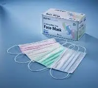
Wearing a mask is a fashion unique, inspires imagination, cultivates the creative spirit, improves school or company image, and dresses stylishly and effectively to prevent covid-19.
1. Type: Diamond shape, 3-ply, non-sterile
2. Size: M, L
3. Color: as photo
4. Outer Layer: Water-repellent non-woven
5. Middle Layer: High level static filtration non-woven
6. Inner Layer: Microfilter Thermal-bond non-woven
7. Nose band: PE iron wire
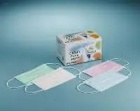
Features
Suitable for OR, ER, patient care area, oral, dental procedure, clinics, isolation, IC practices, patients and other applications.
3-ply, non-woven material, 99% BFE at 3 micron.
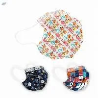
1. Type: Flat shape, 3-ply, non-sterile
2. Size: For kids
3. Color: Green, blue, pink, white
4. Outer Layer: Water-repellent non-woven
5. Middle Layer: High level static filtration non-woven
6. Inner Layer: Microfilter Thermal-bond non-woven
7. Nose band: PE iron wire
4059 6 Layer Hdi F4B Pcb Suppliers
Short on time? Let 6 Layer Hdi F4B Pcb sellers contact you.