Please click here to check who's online and chat with them.

6-Layer Hdi F4B Pcb

Supplier From China
Mar-29-12

Special futures
Thickness: 1.6mm
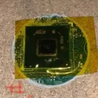
Application: projector or projecting apparatus
Minimum trace size: 0.1mm
Minimum drill: 0.15mm
With blind and buried holes
Layers: 1 to 28
Board finished thicknesses: 0.2 to 7.0mm
Materials: FR-4, CEM-3, high Tg, halogen-free FR4 and Rogers,F4B
Maximum finished board size: 580 x 900mm
Minimum hole size: 4mil (0.1mm)
Minimum trace width/space: 3.5/3.5mil
Surface finishes/treatments: HASL, lead-free HASL, immersion gold, gold plating, immersion silver, immersion tin and OSP
Copper thicknesses: 0.5 to 6oz
Solder mask colors: green, yellow, black, white, red and blue
Copper thickness in hole: >18um
Inner packaging: plastic bag (vacuum packing)
Outline tolerance: ¡À0.13mm
Hole size tolerance: (PTH) ¡À0.076 and (NPTH) ¡À0.05mm
With UL and TS16949:2002 marks
Special requirements: buried and blind vias, impedance control, via plug, BGA soldering and gold finger
Profiling: punching, routing, V-cut and beveling
OEM services to all sorts of printed circuit board assembly as well as electronic encased products are provided.

Inner:vacuum packaging.
Outer:carton.

Price and Minimum Quantity

Price: Negotiable
MOQ: Not Specified

Recent User Reviews

This user has not received any reviews yet!

Verification Status


Contact Supplier
Renew

More Items Similiar to: 6-Layer Hdi F4B Pcb

GOLD Member
May-13-20
Supplier From Garfield Heights, Ohio, United States
 
We just processed in a large batch of chipsets. I posted below current inventory and attached pictures of each type of chipset. Please review and let me know your interest/offer.

Chipset 1 (H61) â?? 3,350 units
Chipset 2 (H81) â?? 2,206 units
Chipset 3 (H55) â?? 436 units
Chipset 4 (B250) â?? 1,600 units
Chipset 5 (SR406) â?? 345 units


Thank you,

Divanti Group
GOLD Member
VERIFIED
Apr-06-21
Supplier From Jamnagar, Gujarat, India
 
we are leading manufacturer & exporter of standoff/spacers as per requirement or Drawing
GOLD Member
Oct-05-24
Supplier From Chon Buri, Thailand
 
Hankook Smart Flex AH35

FEATURES AND BENEFITS

All weather traction
Enhanced controllability
Fuel efficient drive
Excellent durability


The Hankook Smart Flex AH35 is a highway terrain all-season tire manufactured for commercial vehicles. The tyre model is made to be mounted on the vehicle's steering axle.

Hankook Smart Flex AH35 - Key Features

All-Weather Performance: The tire offers reliable traction in dry, wet, and winter conditions, thanks to its wide grooves and 3D sipes, which also prevent hydroplaning.
Enhanced Control: The ribbed tread design ensures constant road contact, improving steering response and driving stability.
Fuel Efficiency: The optimized 3D siping reduces rolling resistance, leading to lower fuel consumption and CO2 emissions.
Durability: Reinforced carcass structure maintains the tire's shape under heavy loads, extending tread life and making it cost-efficient.
Jul-14-20
Supplier From Shenzhen, Guangdong, China
 
Layer count: 10 layer
Board thickness 0.80mm
Raw material FR4 370HR
Min.line width/space 0.075/0.075mm
Minimum hole diameter 0.10mm
Surface finishing ENIG
Plug via-in-pad by resin and plate flat
Jul-14-20
Supplier From Shenzhen, Guangdong, China
 
Layers3 36 Layers

HDI Step 3+N+3

Min.Line Width0.05mm (2 mil)

Min.Line Space0.05mm (2 mil)

Min.Annular ring0.1mm (4 mil)

Min. Via0.1mm (4 mil)

Max.Size500mm X 800mm

MaterialFR4,High Tg220

Material thickness Start at 25um Plus copper

Copper thickness0.3 OZ to 10 OZ (10um 350um)

Please contact us for more information about HDI PCB Board.
Feb-12-20

6 Layer Hight Pcb

$1
MOQ: Not Specified
Supplier From Shenzhen, Shenzhen, China
 
6 layer hight PCB, OEM design PCB
1) Thickness: 0.1mm-5mm
2) Minimum linewidth:0.075mm/3mil
3) Minimum gap:0.065/2.8mil
4) Minimum aperture inradium:0.15mm
5) Minimum aperture external diameter:0.45mm
6) Minimum BGA:0.2mm
7) Layer 6 layers through hole non-impedance 
All multilayer boards are printed with 36t screen, the resistance welding oil is 50 tons thicker than the traditional 43t, which provides reliability guarantee for the bga and more precise fine lines.
Apr-23-16
Supplier From Shen Zhen, Guang Dong, China
 
Minimum line width/space: 4mils
Surface finish: immersion gold
Board thickness: 1.60MM
Minimum drilled hole diameter: 10mils
Copper thickness: 0.5oz
Oct-22-11
Supplier From Guangdong, Shenzhen, China
 
Our PCB Production Capability for your reference
1) Layer: from 1 to 20
2) Board finished thickness: 0.5-6.0mm
3) Material: FR-4,CEM-1, CEM-3, High TG, FR4 Halogen Free, etc
4) Surface finish/treatment: HASL/HASL lead free, HAL, Chemical Gold/tin, Immersion Silver/Gold/Tin, OSP,
Gold plating, Hard &Soft gold, Plating tin.
5) Product range: Flex-PCB, Rigid-PCB, Flex-rigid PCB,HDI PCB ,PCB of single,
Double and Multi-layers, High frequency PCB ,etc
6) Max. finished board size: Single & Double Layer:450mm*650mm
Multilayer:450*500mm
7) Min. drilled hole size: 3mil(0.075mm)
8) Min. line width: 3mil(0.075mm)
9) Min. line spacing: 3mil(0.075mm)
10) Solder mask color : Green/yellow/black/white/red/blue
11) Copper thickness in hole: >20.0um (1mil)
12) Shape tolerance: plus or minus 0.13
13) Hole tolerance: PTH: plus or minus 0.076; NPTH: plus or minus 0.05
14) Certificate: UL,ISO9001,ISO14001,SGS,RoHS compliance
15) Special req. Buried and blind vias +controlled impedence +BGA
16) Profiling : Punching ,Routing ,V-CUT, Beveling.


Inner: Vacuum packing/Plastic bag
Outer: Standard carton packing.
Jun-19-20

Hdi Pcb

$1
MOQ: Not Specified
Supplier From Hangzhou, Zhejiang, China
 
What is HDI PCB
High density interconnect (HDI) PCB, represent one of the fastest growing technologies in PCBs. Because of its higher circuitry density than traditional circuit boards, the HDI PCB design is able to incorporate smaller vias and capture pads, and higher connection pad densities. HDI Boards contain blind and buried vias and often contain micro vias of 0.006 or less in diameter.
By using HDI technology, designers now have the ability to place more components on both sides of the raw PCB if desired. Now as the development of via in pad and blind via technology, it allow designers to place smaller components closer together. This means faster transmission of signals and a significant reduction in signal loss and crossing delays.
HDI PCB is regularly found in mobile phones, touch-screen devices, laptop computers, digital cameras, 4G network communications, also prominently featured in medical devices.
Advantages of HDI PCB
The most common reason for using HDI technology is a significant increase in packaging density. The space that obtained by finer track structures is available for components. In addition, overall space requirements are reduced will result in smaller board sizes and fewer layers.
Usually FPGA or BGA are available with 1mm or less spacing. HDI technology makes routing and connection easy, especially when routing between pins.

Verification Status