INDIUM PHOSPHIDE (InP) WAFERS are semiconductor materials made of indium phosphide, a compound semiconductor that is widely used in high-frequency and optoelectronic applications. Due to its efficient electron mobility and direct bandgap properties, InP is favored for devices such as:
High-speed electronics
Laser diodes
Photodetectors
Telecommunications applications, including optical fiber communication
We offer the following InP Wafers:
Undoped InP Wafers: These are pure InP with no intentional doping, used in various applications where intrinsic properties are required.
N-type InP Wafers: Doped with donor impurities (such as tellurium) to increase electron concentration, useful in transistors and high-speed electronics.
P-type InP Wafers: Doped with acceptor impurities (such as zinc) to create holes in the semiconductor, used in light-emitting devices and other optoelectronics.
InP Substrates: Used as a base for growing other semiconductor materials in heterostructures for various applications.
InP Membrane Wafers: Thin layers of InP used for specific applications, including applications in flexible electronics and advanced photonic devices.
InP-based Quantum Dot Wafers: Engineered to create quantum dots that can be used in photonic and optoelectronic devices for enhanced performance.
VFD for biomass burner, biomass gasification burner. For electric cabinet frequency and voltage converting, to meet different countries voltage. Ensure the bioamss burner can work well.
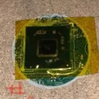
We just processed in a large batch of chipsets. I posted below current inventory and attached pictures of each type of chipset. Please review and let me know your interest/offer.
Chipset 1 (H61) â?? 3,350 units
Chipset 2 (H81) â?? 2,206 units
Chipset 3 (H55) â?? 436 units
Chipset 4 (B250) â?? 1,600 units
Chipset 5 (SR406) â?? 345 units
GaAs Wafers
Gallium Arsenide (GaAs) wafers are critical components in modern electronics and photonics due to their superior electrical and optical properties.
Here�¢??s a focused overview:
GaAs�¢?? is shorthand for Gallium Arsenide, a compound made up of two elements, and the semiconductor used to manufacture GaAs wafers. GaAs is used as a direct bandgap semiconductor, which in layman�¢??s terms, simply means that particles such as electrons can pass through components much quicker and with very little interference. This makes them particularly useful in optical devices because photons, the basic unit for all light, can pass through lenses with ease.
What are GaAs Wafers Use For?
The use of GaAs wafers is dictated by the capabilities of the compound. Because GaAs is a direct bandgap semiconductor, it is especially useful in sensitive electronic equipment that requires amplifying low frequencies. Some of the most common applications for GaAs wafers include:
The Variable Speed Drive FRENIC series is equipped with functions and performance to meet all types of requirements, and in addition it is easily maintained and environmentally friendly. The series lineup ranges from simple to advanced-function models, enabling model choices matching situations for use. Fuji Electric provide Variable Speed Drives perfect for automating and with energy saving devices like a fan pump or carrier and variable speeds.