Supplier : Electronic components, supplier various types of active components, integrated IC, memory chips, the second transistor, and passive components, capacitors, inductors, resistors
Established: 2003
Standards: ISO9001
Verification Status
Contact Details:
B 2202 Jiahe Huaqiang Building, Shenan
Shenzhen
518031
Futian
China
VFD for biomass burner, biomass gasification burner. For electric cabinet frequency and voltage converting, to meet different countries voltage. Ensure the bioamss burner can work well.
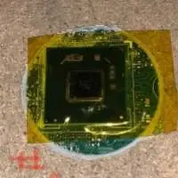
We just processed in a large batch of chipsets. I posted below current inventory and attached pictures of each type of chipset. Please review and let me know your interest/offer.
Chipset 1 (H61) â?? 3,350 units
Chipset 2 (H81) â?? 2,206 units
Chipset 3 (H55) â?? 436 units
Chipset 4 (B250) â?? 1,600 units
Chipset 5 (SR406) â?? 345 units
Bamboo lamp/ Bamboo lantern is made by an experienced craftsman from Vietnam. This unique lamp will make your room more impressive. We have various designs for you.
INDIUM PHOSPHIDE (InP) WAFERS are semiconductor materials made of indium phosphide, a compound semiconductor that is widely used in high-frequency and optoelectronic applications. Due to its efficient electron mobility and direct bandgap properties, InP is favored for devices such as:
High-speed electronics
Laser diodes
Photodetectors
Telecommunications applications, including optical fiber communication
We offer the following InP Wafers:
Undoped InP Wafers: These are pure InP with no intentional doping, used in various applications where intrinsic properties are required.
N-type InP Wafers: Doped with donor impurities (such as tellurium) to increase electron concentration, useful in transistors and high-speed electronics.
P-type InP Wafers: Doped with acceptor impurities (such as zinc) to create holes in the semiconductor, used in light-emitting devices and other optoelectronics.
InP Substrates: Used as a base for growing other semiconductor materials in heterostructures for various applications.
InP Membrane Wafers: Thin layers of InP used for specific applications, including applications in flexible electronics and advanced photonic devices.
InP-based Quantum Dot Wafers: Engineered to create quantum dots that can be used in photonic and optoelectronic devices for enhanced performance.