Dongguan Kam Er Te Electronics Co., Ltd. Was established in 2005, focusing on one-stop production and manufacturing services for electronic products such as SMT surface mount processing/PCBA processing/DIP plug-in post welding/functional testing/finished product assembly, PCBA OEM materials/OEM materials/component procurement.
We just processed in a large batch of chipsets. I posted below current inventory and attached pictures of each type of chipset. Please review and let me know your interest/offer.
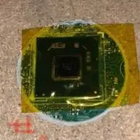
Chipset 1 (H61) â?? 3,350 units
Chipset 2 (H81) â?? 2,206 units
Chipset 3 (H55) â?? 436 units
Chipset 4 (B250) â?? 1,600 units
Chipset 5 (SR406) â?? 345 units
1. RoHS & Lead Free
2. UL & ISO certified
3. Quality & service
4. Quick turn
5. Surface finish: Immersion Gold/HALS/OSP/Gold finger/Carbon print/Peelable mask/Plating gold
6. Solder mask colour: green/white/yellow/blue/red/black
7. Silk screen: white/black/yellow/red/blue/green
8. Applied in industrial facilities/medical facilities/consumer electronics/telecommunications/power supply
We deliver services, not only products.
We offer solutions, not only goods.
Deliver Time For PCB & PCBA
1. PCB production time: sample: 3-4 days / production: within 7 days
2. Fast pcb delivery: 24 hours for 2L ; 48 hours for 4L ; 72 hours for 6L.
3. Component purchase: 2 days if all components is available in our domestic market.
4. PCB Assembly: samples: within 8 days / mass production: within 12 days
INDIUM PHOSPHIDE (InP) WAFERS are semiconductor materials made of indium phosphide, a compound semiconductor that is widely used in high-frequency and optoelectronic applications. Due to its efficient electron mobility and direct bandgap properties, InP is favored for devices such as:
High-speed electronics
Laser diodes
Photodetectors
Telecommunications applications, including optical fiber communication
We offer the following InP Wafers:
Undoped InP Wafers: These are pure InP with no intentional doping, used in various applications where intrinsic properties are required.
N-type InP Wafers: Doped with donor impurities (such as tellurium) to increase electron concentration, useful in transistors and high-speed electronics.
P-type InP Wafers: Doped with acceptor impurities (such as zinc) to create holes in the semiconductor, used in light-emitting devices and other optoelectronics.
InP Substrates: Used as a base for growing other semiconductor materials in heterostructures for various applications.
InP Membrane Wafers: Thin layers of InP used for specific applications, including applications in flexible electronics and advanced photonic devices.
InP-based Quantum Dot Wafers: Engineered to create quantum dots that can be used in photonic and optoelectronic devices for enhanced performance.