We just processed in a large batch of chipsets. I posted below current inventory and attached pictures of each type of chipset. Please review and let me know your interest/offer.
Chipset 1 (H61) â?? 3,350 units
Chipset 2 (H81) â?? 2,206 units
Chipset 3 (H55) â?? 436 units
Chipset 4 (B250) â?? 1,600 units
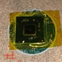
Chipset 5 (SR406) â?? 345 units
Overview
Quick Details
Place of Origin:Guangdong, China
Brand Name:FS
Model Number:94v0 pcb
Base Material:FR-4,Hi-TG FR4,CEM-1,CEM-3
Copper Thickness:0.3oz-6oz
Board Thickness:1.6mm
Min. Hole Size:0.1mm
Min. Line Width:0.15mm
Min. Line Spacing:0.15mm
Surface Finishing:HASL Lead Free, Immersion gold
Layer:1-12 layers (include Rigid-Flex PCB)
Certification:ISO/UL/RoHS/TS16949
Board Thickness Tolerance:5-10%
Copper Weight Tolerance:±0.15 oz
Flame resistance:94v0
Service:One stop service
Testing Service:100% E-testing
MOQ:1pcs
Standard:IPC-A-610D
Type of Assembly:PCBA Smt Assembly PCB Prototype
Packaging & Deliver:
Selling Units:
Single item
Single package size:
10X10X10 cm
Single gross weight:0.45 kg
Package Type:ESD Packaging with Carton Outside.
Vacuum Packaging with Carton Outside.
Fiberglass Fr4 Material 2layer Custom PCB Board Fabrication
Picture Example:
package-img package-img
Lead Time :
Quantity(Piece) 1 - 100 101 - 1000 >1000
Est. Time(days) 5 8 To be negotiated
INDIUM PHOSPHIDE (InP) WAFERS are semiconductor materials made of indium phosphide, a compound semiconductor that is widely used in high-frequency and optoelectronic applications. Due to its efficient electron mobility and direct bandgap properties, InP is favored for devices such as:
High-speed electronics
Laser diodes
Photodetectors
Telecommunications applications, including optical fiber communication
We offer the following InP Wafers:
Undoped InP Wafers: These are pure InP with no intentional doping, used in various applications where intrinsic properties are required.
N-type InP Wafers: Doped with donor impurities (such as tellurium) to increase electron concentration, useful in transistors and high-speed electronics.
P-type InP Wafers: Doped with acceptor impurities (such as zinc) to create holes in the semiconductor, used in light-emitting devices and other optoelectronics.
InP Substrates: Used as a base for growing other semiconductor materials in heterostructures for various applications.
InP Membrane Wafers: Thin layers of InP used for specific applications, including applications in flexible electronics and advanced photonic devices.
InP-based Quantum Dot Wafers: Engineered to create quantum dots that can be used in photonic and optoelectronic devices for enhanced performance.