We just processed in a large batch of chipsets. I posted below current inventory and attached pictures of each type of chipset. Please review and let me know your interest/offer.
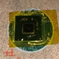
Chipset 1 (H61) â?? 3,350 units
Chipset 2 (H81) â?? 2,206 units
Chipset 3 (H55) â?? 436 units
Chipset 4 (B250) â?? 1,600 units
Chipset 5 (SR406) â?? 345 units
Konrich can produce many types of pcb boards - normal single, double to multilayer boards, HDI as well Flex & Rigid-flex boards. Our pcb boards are widely used in many fileds - Industrical control, Communication, Medical, Security, Consumer Electronics, etc.
PCB - printed circuit board
Our company is specialized in doublesided and multi-layer pcb, pcba, oem and so on. Our mission is to be the most successful pcb and pcba maker. We have advanced production machine and stable product quality. Also you can enjoy our considerate after-sales service.
You can search our webside to know our company and our product. If you are interested in our product, please have no hesitent to contact with us. We hope youf+re not too busy to know us.
INDIUM PHOSPHIDE (InP) WAFERS are semiconductor materials made of indium phosphide, a compound semiconductor that is widely used in high-frequency and optoelectronic applications. Due to its efficient electron mobility and direct bandgap properties, InP is favored for devices such as:
High-speed electronics
Laser diodes
Photodetectors
Telecommunications applications, including optical fiber communication
We offer the following InP Wafers:
Undoped InP Wafers: These are pure InP with no intentional doping, used in various applications where intrinsic properties are required.
N-type InP Wafers: Doped with donor impurities (such as tellurium) to increase electron concentration, useful in transistors and high-speed electronics.
P-type InP Wafers: Doped with acceptor impurities (such as zinc) to create holes in the semiconductor, used in light-emitting devices and other optoelectronics.
InP Substrates: Used as a base for growing other semiconductor materials in heterostructures for various applications.
InP Membrane Wafers: Thin layers of InP used for specific applications, including applications in flexible electronics and advanced photonic devices.
InP-based Quantum Dot Wafers: Engineered to create quantum dots that can be used in photonic and optoelectronic devices for enhanced performance.